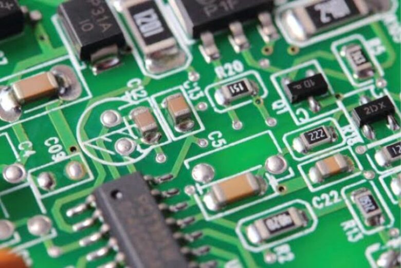
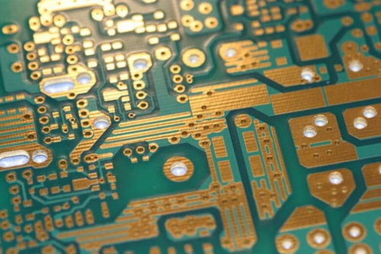
PCB stands for Printed Circuit Board which is the essential part of every electronic device, from simple ones like digital clocks to the more complex ones. PCB directs the electricity on the surface via a network of copper pathways bringing your device to life.
If you have ever wondered how these are made, keep reading this text, because we are going to write step to step guide. However, if you want to learn more about it, in great detail, visit www.pcbonline.com.
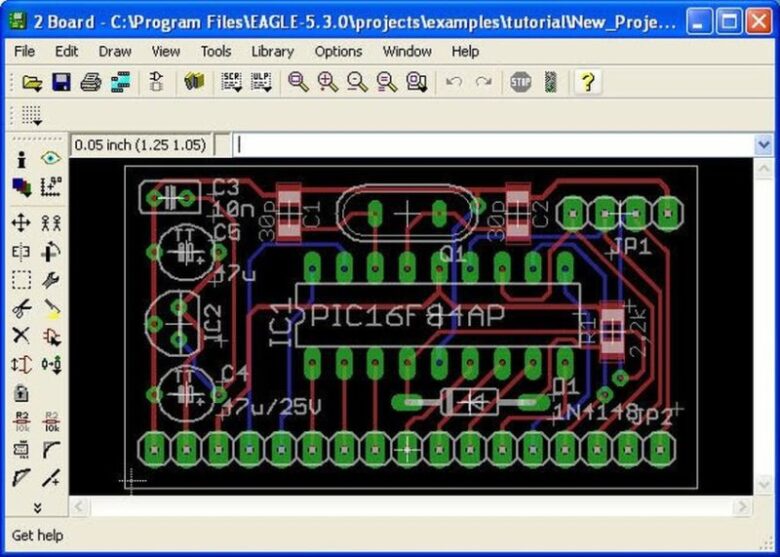
Clearly, the very first thing that has to be done is the design. Depending on the use, the designer uses software called Extended Gerber to create a blueprint. It is also used as an output format because it encodes all the information a designer needs. Once this process is done, the designer checks everything once more to ensure that there are no errors, the design is then sent to PCB fabrication house for production. Upon the arrival DFM (Design for Manufacturer) check is done by the fabricator.
The next step is printing. As you can imagine, a special kind of printer, called plotter printer, is used. It basically makes the photo negative (film) of the board and applies two colors – black and clear ink. Each PCB layer and solder mask has its own film which means that the two-layer PCB requires four sheets. The perfect alignment is of crucial importance, and to achieve it all the films have to be lined up and a registration hole is punched through them. It is used as a guide in the later steps of the production process.
The PCB design is printed onto a piece of laminate, which is used as structure and copper is then connected to it and engraved in it. The next step is to cover this laminate with the resist (a type of photosensitive film). It is made out of chemicals that harden when exposed to the ultraviolet light. With the help of registration holes, the technicians line up the laminate and the resists and exposed it to the ultraviolet light which hardens the certain parts of the resist. Since only areas which will hold the copper have to be modified, the black ink is used to prevent the changes in other parts. Upon the completion of this process, the board is cleaned with an alkaline solution to remove anything that is unnecessary.
Furthermore, it is time to remove the unwanted copper. Chemicals are used to clean the copper that is not under the photo resist. Once this is done, the technicians also remove the photo resist which means that only copper necessary for the PCB is left.

Now, those holes are once again used to perfectly align the layers of PCB. The technicians use a so-called optical punch machine. Since after this step the defects on the inner layers cannot be corrected, another machine is used to ensure that there are no faults by comparing the PCB with the original blueprint.
When it is confirmed that there are no errors, the layers have to be laminated by a press that uses both heat and pressure. Finally, the holes have to be drilled, but before this, an X-ray machine is used to locate the exact spots, again using the Extended Gerber as a guide.

The next step is plating. Upon being thoroughly cleaned, the panel is exposed to multiple chemical baths during which the copper is added into all previously drilled holes.
Again, the photo resist is added, but this time only to the outer layer, since it still has to be imaged. Once this process is finished, these layers are plated in tin that has to protect the copper of the outer layer. Now it is time for another etching process when the excess copper is removed. Before adding the solder mask to both sides, the panel has to be cleaned and covered with an epoxy solder mask ink.
We have nearly come to an end. The surface has to be coated with gold or silver and silk-screened which is the process of printing all important information onto the panel. Lastly, the final electrical tests have to be done to ensure that everything is functioning right.


